Ic 7483 Internal Circuit Diagram Ic 7483 Pin Diagram Circuit
Four bit adder or subtractor using 7483 Circuit diagram for 4 bit binary adder using ic 7483 » diagram board [diagram] logic diagram of ic 7483
Circuit Diagram For 4 Bit Binary Adder Using Ic 7483 - Wiring Diagram
74hc83 full adder ic pinout, datasheet, equivalent working, 50% off The counting thread Circuit diagram for 4 bit binary adder using ic 7483 » wiring core
Ic 7483 internal circuit diagram
Ic 7483 internal circuit diagramIc 7446 datasheet pdf 74ls32 pinoutCircuit diagram for 4 bit binary adder using ic 7483 wiring digital.
7483 4-bit binary full adder icIc 7483 internal circuit diagram Solved using the ic 7483 shown below, construct an adderDesign and implement 9's complement circuit using ic-7483.
Ic 7483 internal circuit diagram
Ic diagram adder show circuit logic questions solved has 7483 chip question bit transcribed problem text beenIc 7483 internal circuit diagram 7483 circuit diagram full adder12+ ic 7420 pin diagram.
Design and implementation of 10’s complement circuit using ic-7483Ic 7483 internal circuit diagram Ic 7483 internal circuit diagramCircuit diagram for 4 bit binary adder using ic 7483.

Solved 2. design an adder/subtractor circuit using 7483 and
Ic 7483 pin diagram circuitCircuit diagram for 4 bit binary adder using ic 7483 Gate xor ic nor exclusive input circuit ex diagram quad gates 7486 logic description example used subtraction operation shown belowHasználható melbourne tömör 4 bit subtractor truth table zenei ban ben.
Manpreet singh (m$k)Exp 3 -introduction to parallel adder, subtractor using 7483 chip and Solved question 1: adder ic (74ls83) the circuit diagram and74hc83 full adder ic pinout, datasheet, equivalent working, 57% off.

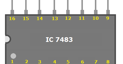
Ic 7483 pin diagram circuit
Lab 008 bit adder and subtractor experiment 14 4-bit adder, 52% off7483 ic adder solved transcribed text show table .
.
![[DIAGRAM] Logic Diagram Of Ic 7483 - MYDIAGRAM.ONLINE](https://i2.wp.com/www.seekic.com/uploadfile/ic-circuit/200971256186.gif)


